
May 22, 2026 / by Dave L - Fortify Labs / In teardown, technical, Hino, Freightliner, Mining, Waste Management, Transport & Logistics, Heavy Equipment
Teardown: Hino & Freightliner
Telematics Module - Part 1
Watching a delivery truck backing up to the Coles loading bay one day got me wondering - “Do these vehicles use the same connected technology as regular cars?”
And if so, what does that mean about how they’re connected? Are they susceptible to cyber attacks? Could a truck be controlled if someone found ways to access them remotely?
After reading some articles about what would happen if these trucks suddenly stopped working, it made me realise just how dependent we are on them. One of these articles from Big Rigs made it clear that without them working around the clock, grocery shelves and fuel supplies would run out surprisingly quickly.
Throughout my journey of digging into automotive systems, one of the components I find the most interesting is the telematics module. It goes by different names (Tbox, TCU, DCM, etc.) but it’s core purpose is the same - to connect the vehicle to the outside world. In this way, it’s like the internet modem sitting in your house.
The Tbox plays a similar role, it provides connectivity to different modules in the vehicle. Without it, features like finding your car on a map, unlocking it remotely, or starting it from your smartphone wouldn’t work.
But, vehicles aren’t only connected for our convenience, they also share diagnostic and historical data about the vehicle itself. And, as I saw from my analysis of the Ford Ranger’s infotainment unit, vehicles can store a great deal of information.
I was curious to see how a Tbox from a commercial transport truck stacks up against ones seen in passenger vehicles. So, we decided to find out. eBay was searched, and 2 commercial Tbox units were purchased from the US. One from a Hino (Toyota’s truck brand) and the other from a Freightliner truck.
This series shows how I approached analysing these Tboxes.
Hino & Freightliner Blog Series
- Part 1: This Post
- Teardown
- PCB Characterization
- Searching for UART, JTAG, and WiFi
- Chip-Off Data Extraction
- Part 2: Obtaining a Useable Image
- Confirming NAND Controller Encoding
- Removing NAND Controller Encoding
- Mounting UBIFS Volumes in Linux
- Part 3: Data Analysis
The Tboxes
As I opened up the shipping boxes, it immediately became apparent that these devices looked nearly identical even though they were from two different manufacturers.
They were also clearly made to endure a harder life than ones I’ve seen in cars. Where those are often made of plastic, these were encased in metal - seemingly to provide more protection during a harder life.
Once I opened the cases, the similarities continued, with the majority of components being identical. This was interesting for a couple reasons:
- Whatever I found one one device could potentially be applied to the other.
- It gave me a way to compare the two, and if required (…which it was…) use one as a sacrificial lamb for testing or pulling apart.
Below we can see how similar these two devices are:
Device Details
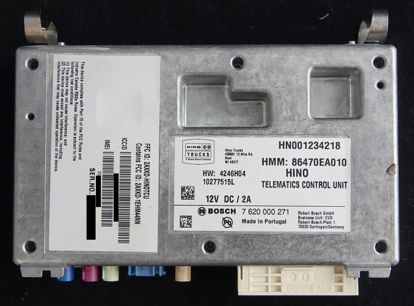
Hino Telematics Control Unit:
- Make / Manufacturer: Bosch
- Part Number: 7 620 000 251
Freightliner Telematics Control Unit:
- Make / Manufacturer: Bosch
- Part Number: 7 620 000 353
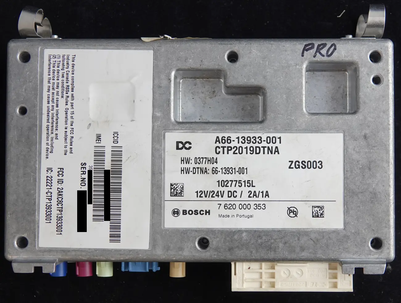
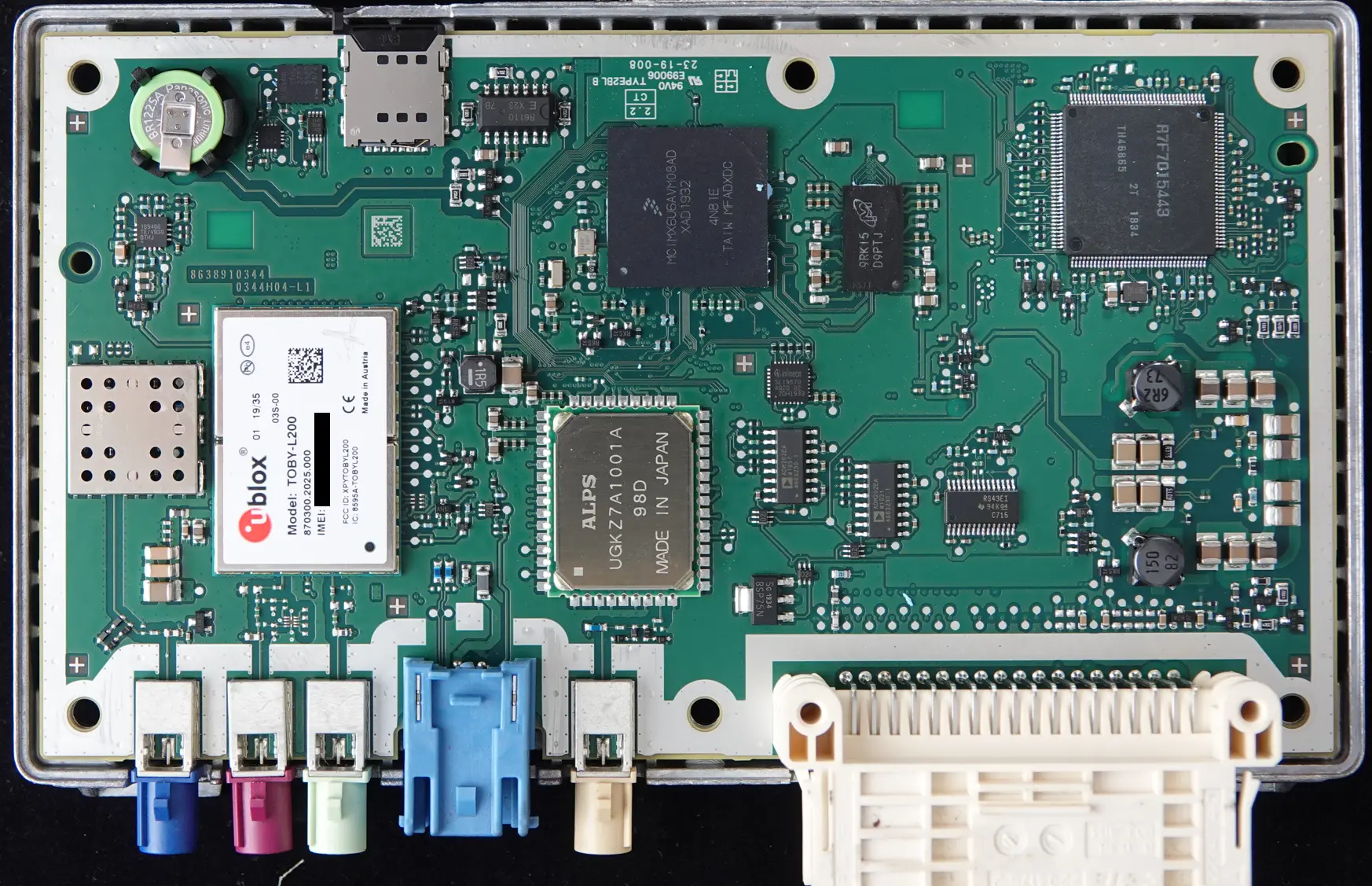
Because these boards were nearly identical, I’ll only show images from the Hino Tbox from this point on.
Physical Examination & Characterising the Board
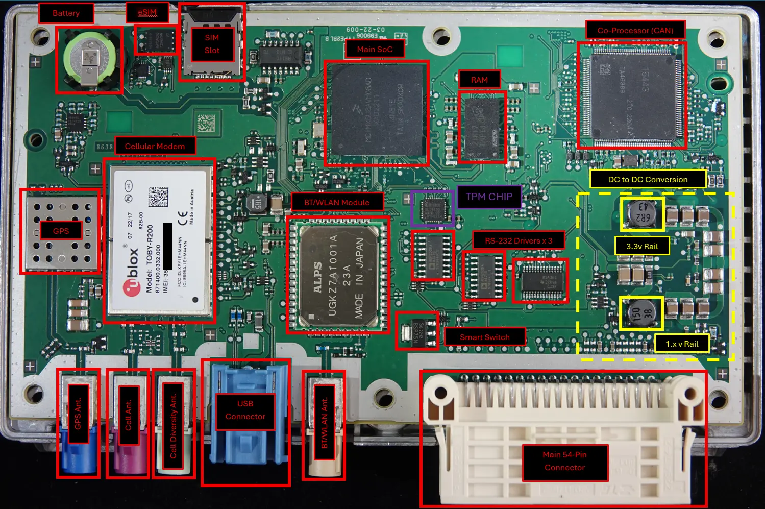
Once opened up, I started to look at what chips were installed on each of their circuit boards.
This gave me a chance to get familiar with how things are laid out and by looking at the chips, I can start to get an understanding of what functionality the Tbox has.
I could see:
- The main processor
- The main storage (flash memory)
- That the board could process CAN data
- That it has GPS onboard
- That it had a cellular modem
- That it had WiFi and Bluetooth capabilities
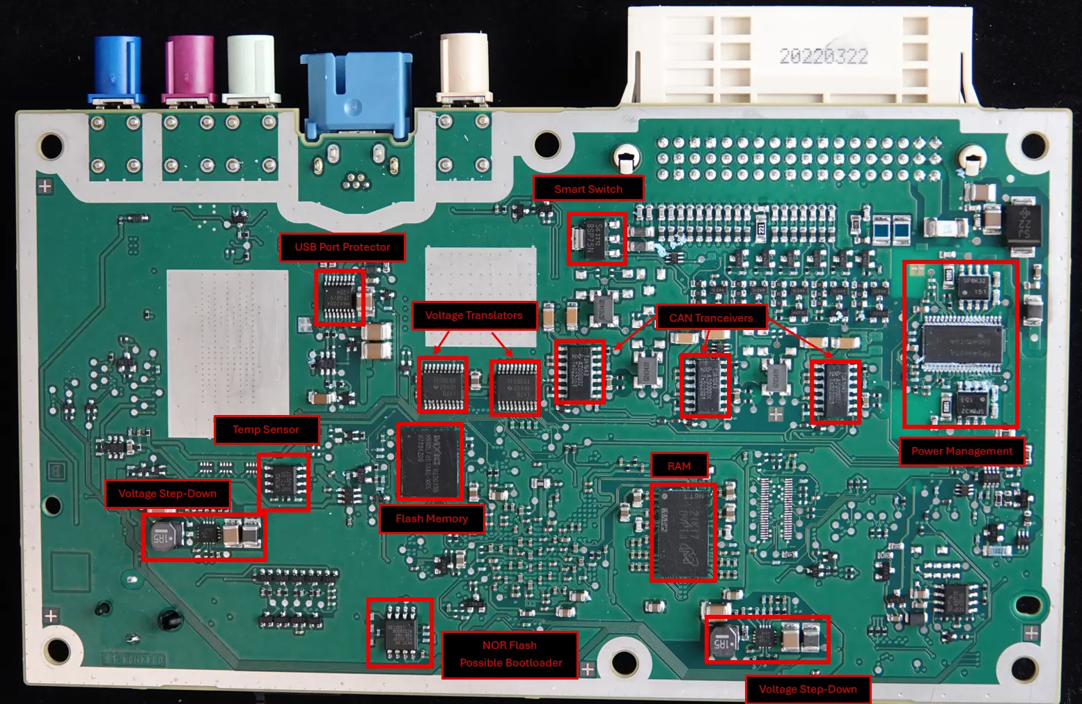
It had all the components needed to connect the vehicle to the outside world (cellular, WiFi, and Bluetooth) but was also conected to the vehicle’s main controller network (CAN). Already, this confirmed that this component provides both a connection to the Internet as well as to an internal network used to control a vehicle.
I now had a pretty good idea of what the Tbox could do. Next up was trying to talk to some of the chips, but in order to to that, I had to figure out how to power it up.
Identifying Power connections
These Tboxes were purchased off eBay, so I wasn’t able to examine the vehicle’s connector to determine what the pins on the connector might be used for.
Therefore, I had to refer back to my board characterisation to try and identify where the power and ground connections might be so that I could power it on. After some probing I found:
- The ground pin (Pin 37) was relatively easy to find as it had continuity between it and the board’s perimeter ground ring and component shielding.
- The main power pin (Pin 1) was traced to a 2.5A fuse, which provided me with some confidence that I had the right power pin.
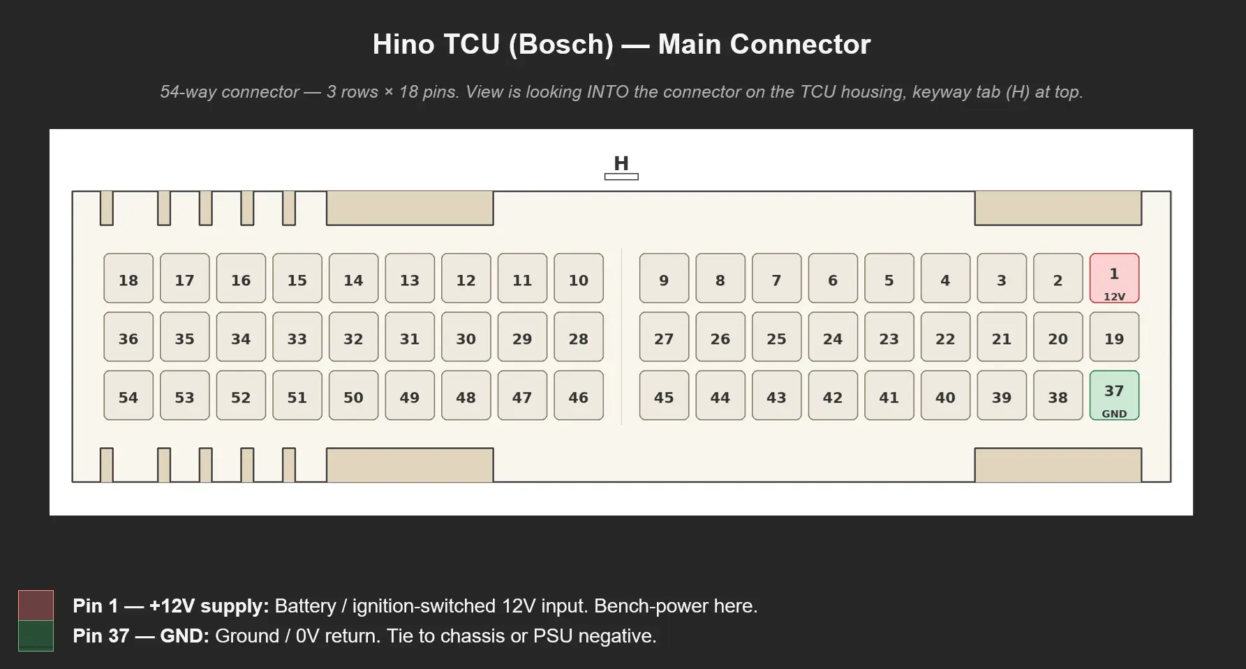
When power was applied (12 V / 2 A - note that this was on the Tbox label), the unit began to draw power. I didn’t let the smoke out, definitely a win!
Now that I had a unit that powered on, I could try and find the right signal lines to talk to the chip(s).
Search for UART
With power sorted, I began probing the board for accessible UART lines.
UART is often used as a debug port that engineers use during a board’s development or programming. It’s normally the first thing we look for when trying to talk to the chips on a board. From that, we might be able to do anything from reading bootloader output and kernel logs, to dropping into a root shell, dumping firmware, modifying boot arguments, or pulling credentials and keys straight out of the running system.
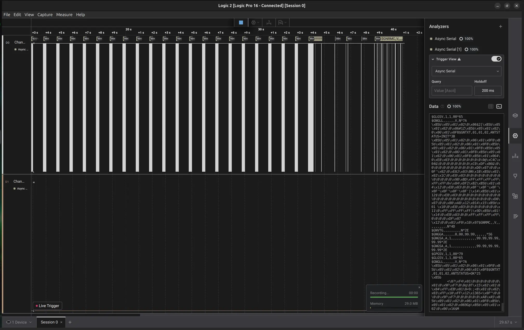
To look for UART interfaces, we used a Saleae logic analyser (Logic Pro 16) and Logic 2 software (v2.4.43) to capture and visualise the digital signals on a board’s test pads.
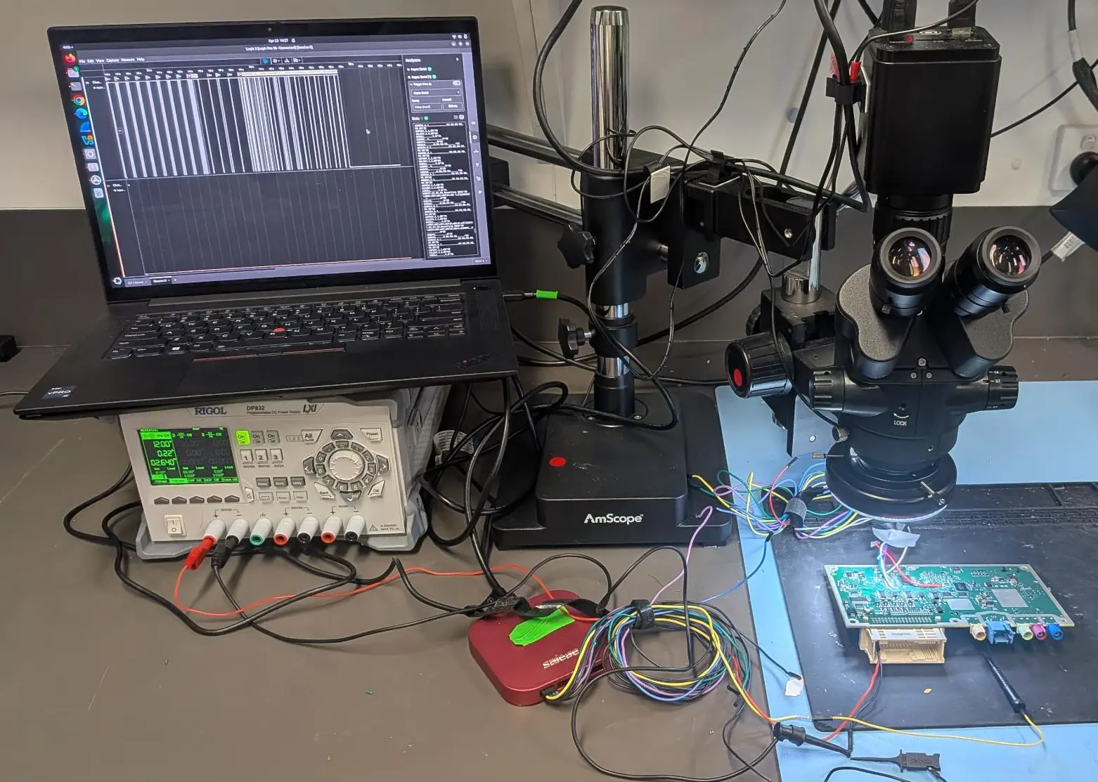
This turned out to be a time consuming, and slightly frustrating process. I ended up probing every test point and component on the PCB with the Saleae to look for digital signals, but ultimately I wasn’t able to find any debug UART interfaces.
I did manage to find a UART signal that appears to be used for GPS functionality, but this did not allow me to communicate with either the processor or cellular modem chips.
Not finding a debug UART might be due to a variety of reasons, including that the interface might not be enabled on production versions, or that the chip needs to be placed in the right mode to enable the UART debug interface, but either way this was a dead end for me.
Here, I show some findings on the GPS UART interface and the work done to try and find UART on the cellular modem.
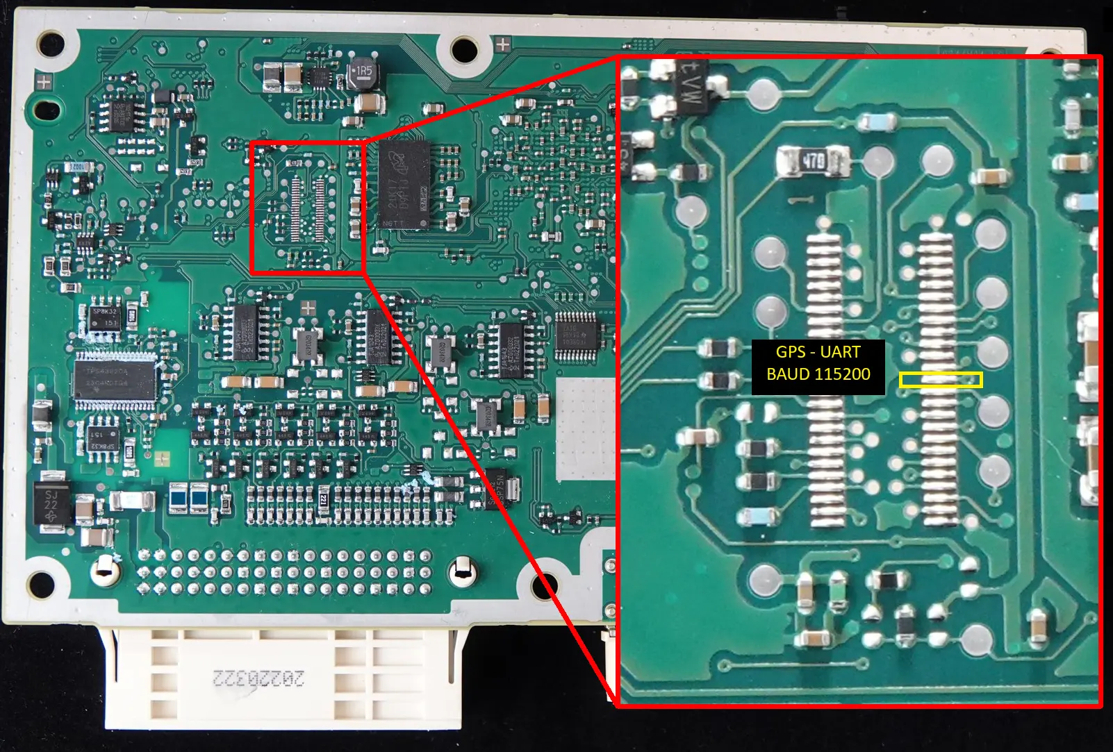
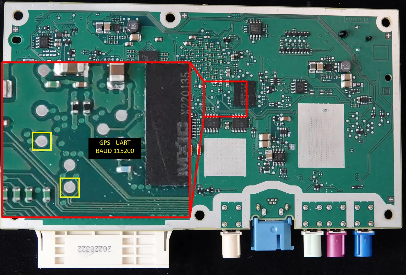
GPS UART
The photos below show the header pins and test pads that showed GPS information.
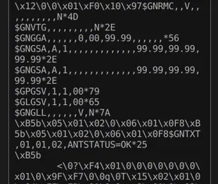
The following screenshot shows the Logic 2 software with Saleae output, including the GPS (NMEA data).
Note: The Saleae was configured to a Baud rate of 115200 bps.
Next, UART on the cellular modem.
Ublox UART
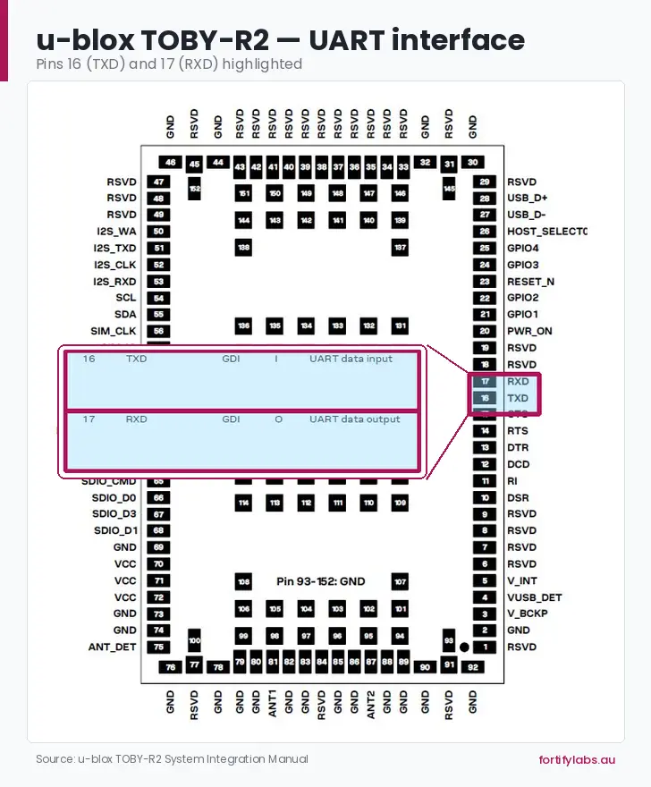
Here I searched for UART interfaces on the Ublox cellular modem module (TOBY-R200).
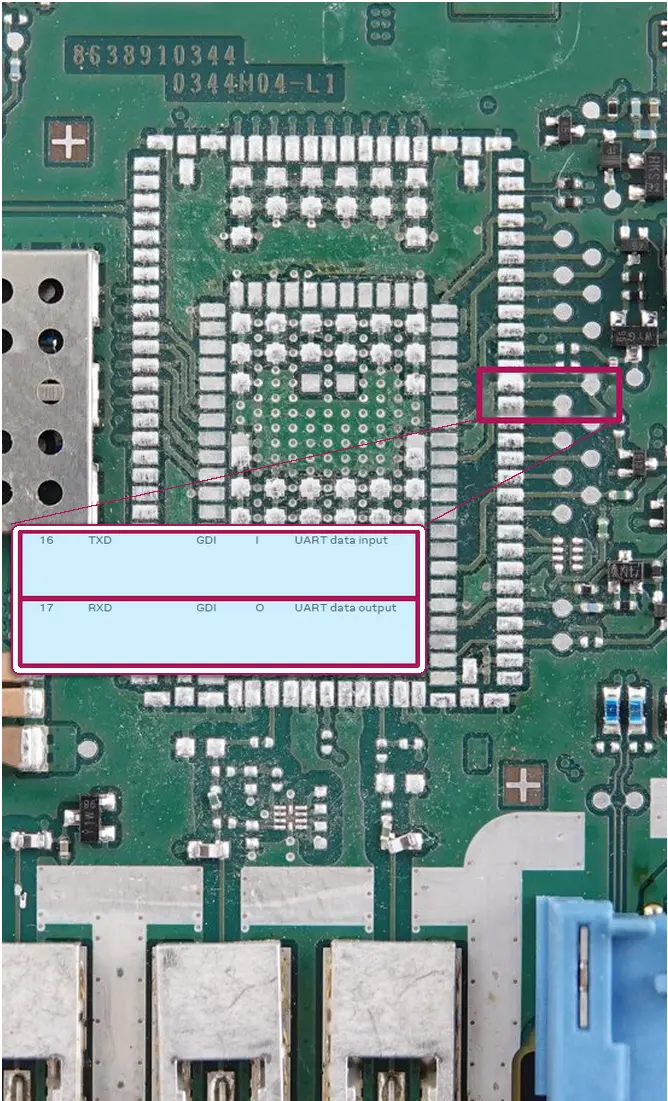
I reviewed the Ublox datasheet which showed that the UART Transmit and Receive pins were located on pins 16 (TXD) and 17 (RXD). Knowing this, and finding a series of test pads located directly adjacent to the Ublox module, pins 16/17 were estimated to be approximately half-way up the module. However, when probed, no digital signals were found that resembled a UART signal.
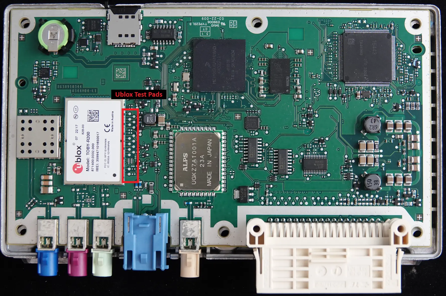
To ensure I was probing the right pins, I removed (chipped-off) the Ublox modem from the Freightliner Tbox to trace the pins and verify them manually. To have a look at our chip-off process see our Komatsu Tbox Teardown.
Note that I verified through both datasheets (TOBY-L200 - Freightliner, TOBY-R200 - Hino) that they shared the same pinout layout.
After physically tracing pins 16 & 17 to the test pads, I confirmed that the ones probed on the Hino board was correct. This confirmed that I was probing the right pins, but that a UART interface did not appear to be active.
As with the processor’s debug UART interface, it is possible that the Ublox UART interface is not configured or that Tbox was not in the right mode.
With my search for UART interfaces at a dead-end, I moved on to looking to see if there were any other ways of communicating directly with the chips on the board.
JTAG Search
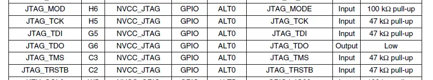
I re-focused, and looked for JTAG pins. As opposed to UART, the JTAG pins were clearly defined in the datasheet.
JTAG is a low-level debug interface that engineers use to test, program, and debug chips development and manufacturing. It’s another high-value target during an assessment because if we can find an unlocked JTAG port, we get direct hardware-level control of the processor.
First, I had to find the right pins and the datasheet pointed me in the right direction.
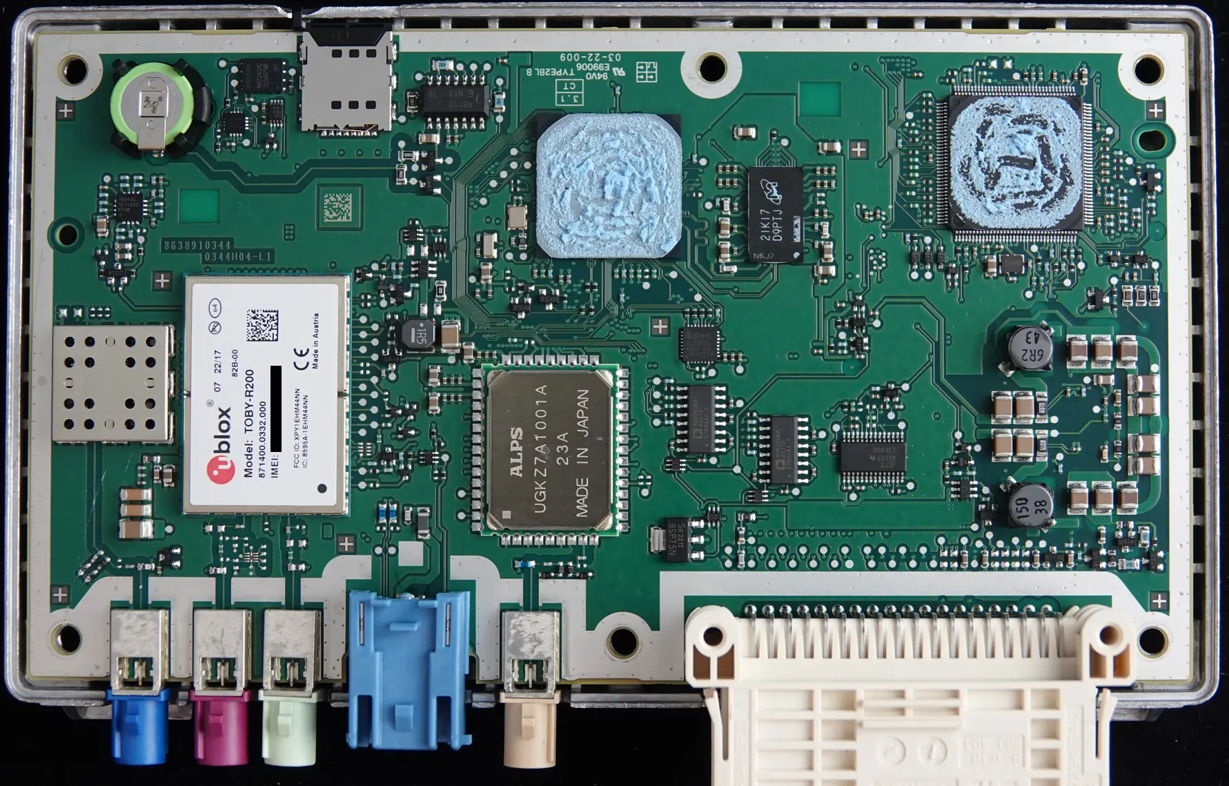
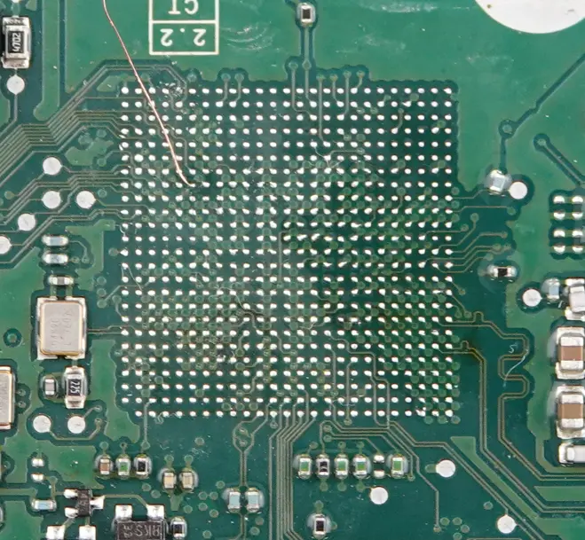
In order to identify JTAG test pins on the Hino PCB, I removed the main NXP processor from the sacrificial (Freightliner) board, allowing me to trace pad locations.
Through this tracing exercise, I found that the test pins for the JTAG pins were routed to an unpopulated debug header.
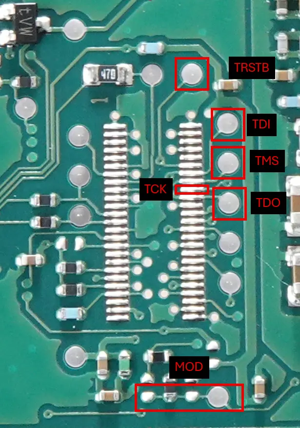
Initial voltage measurements looked promising - the JTAG power rail was live at 3.3V, and the boot mode pin was sitting low, which should put the chip into a JTAG-accessible state.
Using a Segger JLink (ver 11.0) and the J-Link Software (SEGGER J-Link Commander V9.34a), I used the following command
JLinkExe -if JTAG -speed 1000
However, all attempts to connect with the J-Link failed, with the JTAG controller not responding, as seen below:
  user@user-Ub24-Ext:/opt/SEGGER/JLink$ JLinkExe -if JTAG -speed 1000
  SEGGER J-Link Commander V9.34a (Compiled Apr  9 2026 18:20:53)
  DLL version V9.34a, compiled Apr  9 2026 18:19:45
  Connecting to J-Link via USB...O.K.
  Firmware: J-Link V11 compiled Apr  1 2025 10:02:30
  Hardware version: V11.00
  J-Link uptime (since boot): 0d 01h 52m 47s
  S/N: XXXXXXXX
  License(s): GDB
  USB speed mode: High speed (480 MBit/s)
  VTref=3.349V
  Type "connect" to establish a target connection, '?' for help
  J-Link>connect
  Please specify device // core. Default: MCIMX6U5
  Type '?' for selection dialog
  Device>
  Device position in JTAG chain (IRPre,DRPre) Default: -1,-1 => Auto-detect
  JTAGConf>
  Device "MCIMX6U5" selected.
  Connecting to target via JTAG
  TotalIRLen = ?, IRPrint = 0x..000000000000000000000000
  Failed to identify target. Resetting via Reset pin and trying again.
  TotalIRLen = ?, IRPrint = 0x..000000000000000000000000
  Error occurred: Could not connect to the target device.
  For troubleshooting steps visit: 'https://kb.segger.com/J-Link_Troubleshooting'
From this output, it looks like the JTAG is locked down. From the cybersecurity professional in me, this was great to see. From the hacker in me, it was another dead-end. Kudos to Bosch on thwarting my attempts thus far!
Not being able to find methods to communicate directly with the chips, I moved on to other connection paths.
Search for WiFi / BT
I knew from the board characterisation that the Tbox has the right chips in place for WiFi and Bluetooth, so I power cycled it several times to see if would give off any WiFi or Bluetooth signals. I was hoping to find a different way to connect with the Tbox using wireless methods.
However, the Tbox did not send out either signal. Once again, it is possible that the Tbox might not be in the right mode or that WiFi and/or Bluetooth is only used at certain times for for specific functions.
Lack of a Surrogate Vehicle
The ideal scenario would have been to have access to a vehicle with the Tbox installed. Having had access to this, I could have seen how it operates in it’s normal state and baseline it’s behaviour, identify specific signal pins on a working connector, and capture CAN traffic.
Some modern vehicle ECUs (Tboxes, Head Units, etc.) sometimes only fully boot when it receives specific CAN messages. It’s possible that this is the scenario I was facing here, but without access to a surrogate vehicle, this becomes significantly harder to determine. As I didn’t have the budget to buy a complete Hino or Freightliner truck, these questions remain unanswered… for now.
If anyone has one of these trucks, feel free to get in touch, we’d love to have a crack!
Unsuccessful, I moved onto more drastic measures and decided to have a closer look at the device’s memory.
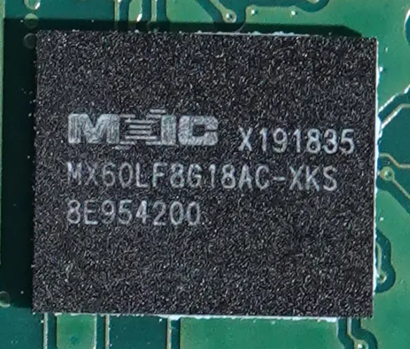
Memory Image - NAND Flash Memory Extraction
Going back to the board characterisation work, I knew which chip likely acted as main storage. If I could read the memory and be able to see it’s filesystems, it could provide a way to dive deeper into it’s functionality, find interesting things, and give possible clues on how else we might be able to interact with the Tbox.
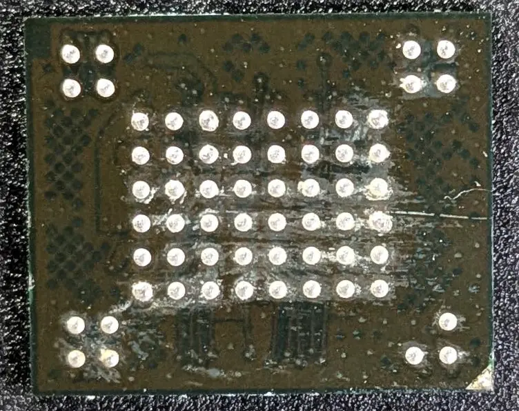
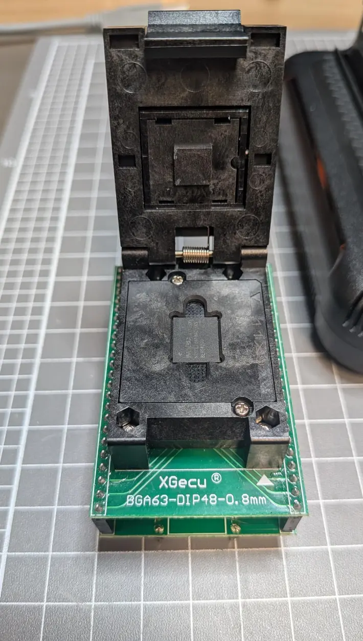
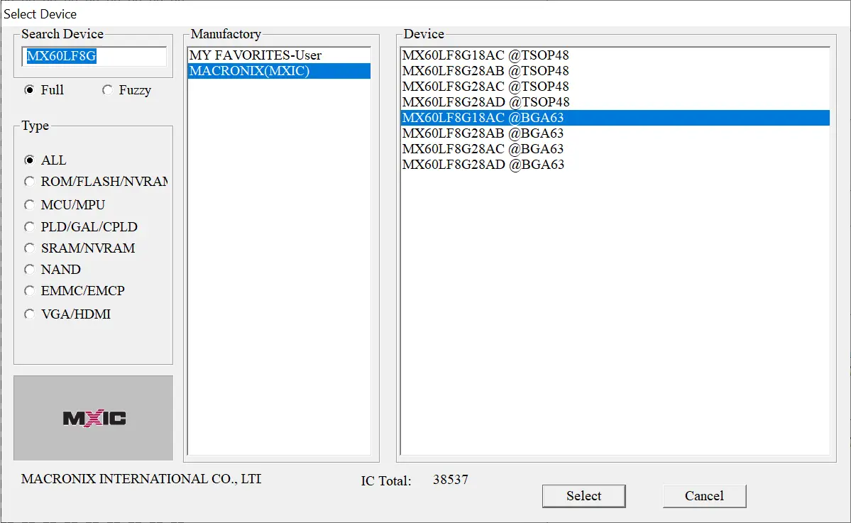
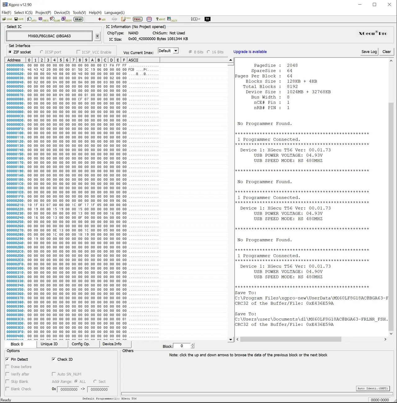
Using a re-work station I removed the NAND Flash Memory (Macronix MX60LF8G18AC chip) from the board.
With the chip removed, it was placed into our XG Zif BGA63 Adaptor & Caddy (XG-BGA63-0.8 / BGA63-DIP48-0.8mm) purchased from AliExpress, and connected to our XGecu universal device programmer (T56).
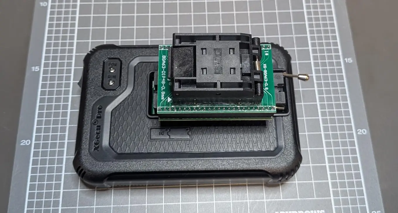
Using the Xgpro Software (v12.90), we selected the right chip and read the chip’s memory.
Conclusion
With this memory image now in hand, I moved on to performing a memory analysis to see what I could find about the operating system, log files, functions, credentials, or historical data kept on the device.
As I’d find out, it wasn’t as easy as I hoped…
Please follow along in Part 2: Obtaining a Useable Image and Part 3: Data Analysis, where we dig into the data we recovered.
Disclaimer
This analysis is based on our professional experience and reflects our best interpretation at the time of examination.
Anyone choosing to replicate these procedures does so at their own risk.
Disassembling a vehicle (or equipment) and interacting directly with its electronic components carries an inherent risk of damage to the equipment. Fortify Labs does not guarantee that any procedure described will be free of risk, nor do we accept responsibility for any resulting damage.